Environmental Scanning Electron Microscope (ESEM)
A scanning electron microscope (SEM) images the sample surface by scanning it with a high energy beam of electrons in a raster scan pattern. It permits analyzing the surface texture of solids and the characterization of powder samples. Its magnification of max. 1:1000000 x exceeds significantly the possibilities of normal light microscopy which is limited due to the wavelength of the visible light (400-800 nm) while the wave length of electrons is just about 0.008 nm.
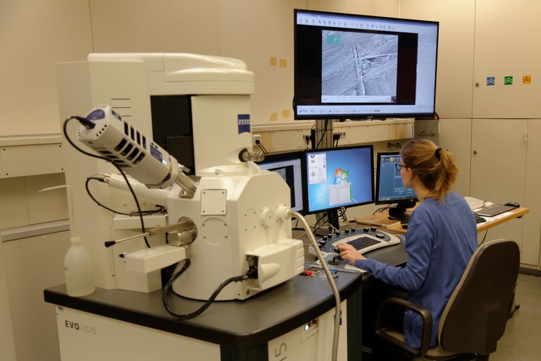
The institute’s Zeiss EVO LS15 has a big sample chamber for maximum specimen heights of 145 mm. It is equipped with a nine fold sample changer which permits quick subsequent investigation of various samples. The SEM operates with variable pressure ranging from common high pressure down to the low pressure range (10 to 3000 Pa). Moist samples like e.g. hydrating binder can be in investigated in the environmental scanning electron microscope (ESEM). Thus an ultrathin sputtering with gold or carbon can be avoided which enables the visualization even of very fine structures like crystals of cement hydrates.

Figure: Environmental scanning electron microscope with attached EDX system on the left

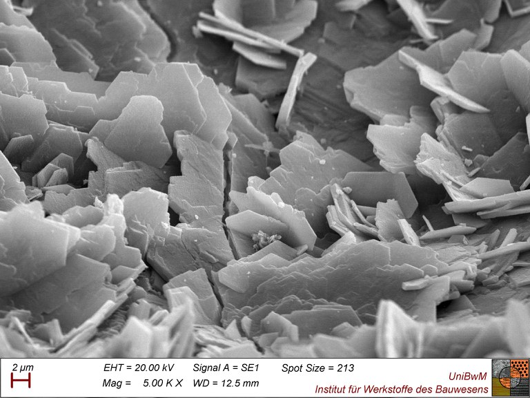
Figure: Portlandite crystals in an air void (5000x magnification)
Energy dispersive X-ray analysis (EDX)
Energy dispersive X-ray analysis (EDX) extends further the experimental opportunities of the SEM. The system uses the characteristic X-rays of atoms as additional secondary signal for a chemical element analysis of the sample surface. The attached Oxford Instruments X-MaxN 50 EDX-system has a SDD-detector (Si(Li)-detector) with an detector area of 50 mm2.

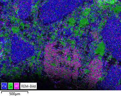
Figure: EDX element mapping of a sand-lime brick sample. For better orientation the X-ray figure is superposed.