Scanning positron microscopy
Based on a pulsed positron beam of variable energy, a scanning positron microscope was developed and built at the institute. This system, the first of its kind in the world, generates a pulsed, monoenergetic positron beam of 1 mm diameter that can be rastered over an area of 0.6 mm x 0.6 mm. The beam pulsing (100 ps pulse width) allows positron lifetime measurements to be made on microstructures (1 x 1 x 0.1 µm3) and near-surface and deeper regions to be scanned by varying the positron energy between 500 eV and 25 keV. The measured positron lifetimes and their intensity provide information about the defect state of the microscopic three-dimensional regions. This opens up non-destructive investigations of defect structures in areas of microscopic dimensions for the first time. A conventional scanning electron microprobe is also integrated into the system, in order to obtain an image of the surface structure of the sample.
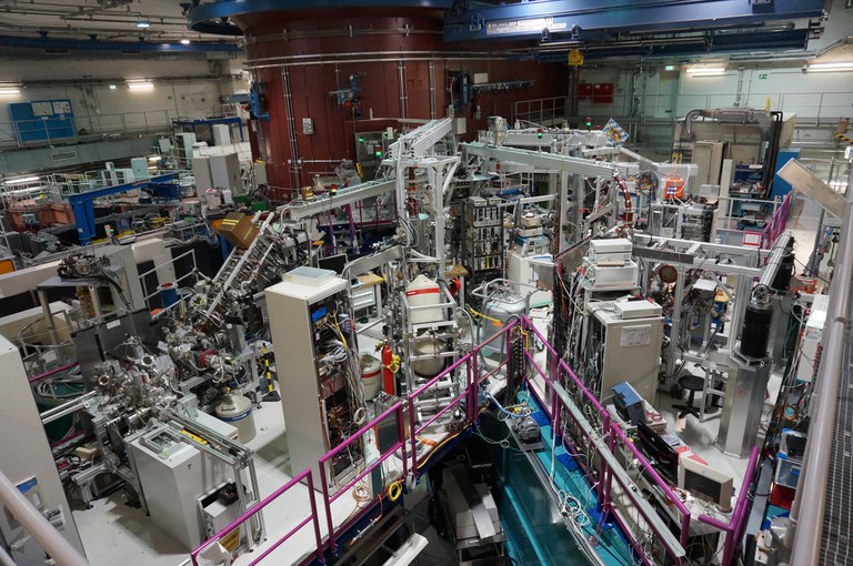
Reactor-based positron source
At the research reactor FRM-II, an intense source of low-energy positrons was developed and built. From the capture of thermal neutrons in the isotope 113Cd, photons in the energy range of a few MeV result. Electron-positron pairs are generated in a platinum foil via pair formation. The average kinetic energy of the positrons is 800 keV. After deceleration to thermal energies and diffusion to the surface, a part of the positrons is emitted with an energy approximately equal to the work function of this material. Thus, a positron beam can be formed by a suitable arrangement and focusing and guided out of the reactor region by a magnetic guide field. The achievable positron intensity scales with the thermal neutron flux at the location of the cadmium. At a thermal neutron flux of 1012n/cm2s, a positron intensity of 108 positrons per second was achieved. This enables novel investigation possibilities of solid surfaces with Auger electron spectroscopy induced by positron annihilation.
Defect structures in metals, alloys and semiconductors
Positron lifetime spectroscopy is used to study manufacturing- and radiation-induced defects, as well as their dynamics and interactions. Positrons from radioactive decays are used as probes to study these defects with atomistic dimensions. From lifetime measurements, information can be obtained on the nature, size, and frequency of these defect structures, which are important for material problems in reactor technology and semiconductor devices. With a pulsed, monoenergetic positron beam apparatus with variable positron energy (positron beam diameter 4 mm), which was developed and set up at the institute for the first time worldwide, defect structure investigations on thin metal layers, on semiconductors, on semiconductor layer structures and interfaces, as well as on high-temperature superconducting single crystal layers, are carried out non-destructively.